You’ve heard the story: a couple of scientists discovered graphene when they repeatedly pulled a strip of adhesive tape off a layer of graphite. Graphene has been all the rage due to its incredible strength, low weight, and electronic properties, but it’s not the only material of its kind. There are plenty of other 2D materials to consider for electrical applications — some of which may work together with graphene, and others that can be used in its place.
Natural Graphene
Graphene has a slew of benefits and unusual material properties. To use the same comparisons as my colleague Dan did in his previous blog post, graphene is about 200 times stronger than steel and has a higher electrical and thermal conductivity than copper. Dan attributes the high electrical and thermal conductivity to its high room temperature electron mobility of greater than 15,000 cm2/(V-s), and up to 200,000 cm2/(V-s) in certain forms. An IEEE Spectrum article from earlier in the year put that last part in simple terms:
“At low temperature, for example, electrons can zip through the material 100 times as fast as they do in silicon for a given voltage.”
Additionally, like I mentioned earlier, the material also weighs very little — less than 1 milligram per square meter, in fact. All of this makes natural graphene a great option for creating fast RF transistors and other electronics.

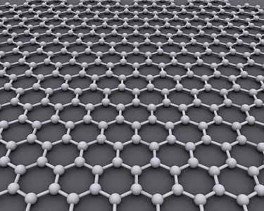
Graphene. Image attributed to AlexanderAIUS.
Having said all that, graphene in its natural state is not entirely without limitations. As we can see in the IEEE Spectrum article, natural graphene does not have a bandgap (or a threshold for electronic excitations) like semiconducting materials do, meaning you cannot turn the current flow off. As you may already know, being able to make switches in currents is important for making logic, which is why semiconducting silicon has been so popular for modern electronics.
What about the research that’s on track to introduce bandgaps to graphene? We might not quite be there yet, according to the article I mentioned. A bandgap can be introduced by stacking layers of the material on top of one another or by cutting it into nanoribbons, although they say this will typically bring forth an important side-effect: reduced electron speed.
Other 2D Materials
While graphene research and manufacturing is well underway and widely talked about, there are other 2D materials out there that have not been explored as thoroughly yet but do show promise, on their own or in combination with graphene.
Boron Nitride
Take boron nitride, for example. Whereas graphene has no bandgap, boron nitride has a very wide bandgap — the same as diamonds. The bandgap is so large that it is not appropriate for switches, but instead it makes for a good insulator. Advancements have been made in terms of combining this material with graphene to create incredibly thin circuits.

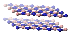
Boron nitride.
Silicene
A competitor to graphene, silicene is a one-atom thick version of silicon that can be grown on silver surfaces. With some similar material properties to graphene (like massless Dirac fermions, for instance), silicene takes it one step further with lower group symmetry and stronger spin-orbit coupling, perhaps making it better suited for integrating with silicon-based electronics than graphene.

Silicene. Image attributed to Ayandatta.
Stanene
Using simulation tools, researchers recently combined 2D monolayers of tin with fluorine atoms to produce what they call stanene, a material that appears to be very similar to graphene. The researchers project that stanene will be able to conduct energy at 100% efficiency along its edges at room temperature, while its center behaves like an insulator. Four lanes of zero-resistance data traffic is supposedly supported, two lanes going in opposite directions along each edge.
In other words, the material is thought to act like dual, side-by-side superconducting wires. There is a fascinating difference between this new material and a normal conductor in terms of resistance. Whereas with a normal conductor, a longer wire would provide a larger resistance, but when it comes to stanene it’s all about where the end-points are in contact with the chip circuitry, resulting in a resistance that remains constant regardless of length.
The researchers are still awaiting experimental confirmation on their new material, but if it is indeed confirmed, stanene could be the next big thing since graphene.
Graphene Research Leads to Accidental Discovery of 2D Glass
The graphene journey has come a long way since that fateful day in 2004. According to gizmag.com, graphene research spawned the accidental discovery of the world’s thinnest glass in 2012. Measuring only two atoms thick, it’s a truly remarkable discovery.
The 2D glass came about when two Cornell researchers grew graphene (via chemical vapor deposition) on a copper film attached to a quartz substrate. When the researchers noted that the graphene layer was discolored, they decided to test it. That’s when they realized that the discolored portion was actually silica glass — in a one-molecule layer. Although they have not yet been able to reproduce these results, the researchers speculate that this type of glass could potentially be used in nanotechnology.
Further Reading
- Check out our graphene blog series from earlier in the year


Comments (0)