A Low-Pass and Band-Pass Filter Using Lumped Elements
Application ID: 15675
Passive devices can be designed using lumped element features if both the operating frequency of the device and the insertion loss of lumped elements are low. This example simulates two types of lumped element filters that are similar to lumped ports, except that they are strictly passive and there are predefined choices for inductances and capacitance.
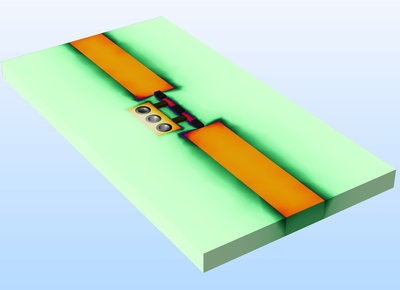
First, a five-element maximally flat low-pass filter is built to compute frequency responses that show the cutoff at the intended frequency. The geometry of each element (surface-mount device, SMD) is simplified as a 2D boundary and the electrical performance is modeled using the Lumped Element boundary condition in the Electromagnetic Waves, Frequency Domain interface. Then, a band-pass filter transformed from the low-pass filter design is simulated in the same frequency range. Both filter models present the S-parameters and electric field distribution.
この model の例は, 通常次の製品を使用して構築されるこのタイプのアプリケーションを示しています.
ただし, これを完全に定義およびモデル化するには, 追加の製品が必要になる場合があります. さらに, この例は, 次の製品の組み合わせのコンポーネントを使用して定義およびモデル化することもできます.
アプリケーションのモデリングに必要な COMSOL® 製品の組み合わせは, 境界条件, 材料特性, フィジックスインターフェース, パーツライブラリなど, いくつかの要因によって異なります. 特定の機能が複数の製品に共通している場合もあります. お客様のモデリングニーズに適した製品の組み合わせを決定するために, 製品仕様一覧 を確認し, 無償のトライアルライセンスをご利用ください. COMSOL セールスおよびサポートチームでは, この件に関するご質問にお答えしています.