DC Characteristics of a MESFET
Application ID: 14999
In a MESFET, the gate forms a rectifying junction that controls the opening of the channel by varying the depletion width of the junction.
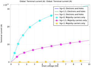
In this model we simulate the response of a n-doped GaAs MESFET to different drain and gate voltages. For a n-doped material the electron concentration is expected to be orders of magnitude larger than the hole concentration. Accordingly, it is possible to use the majority carrier option to compute an accurate solution with less degrees of freedom then it would normally be needed using the electrons and holes formulation.
The agreement between the two methods is excellent, but the majority carrier formulation solves twice as fast.
この model の例は, 通常次の製品を使用して構築されるこのタイプのアプリケーションを示しています.
ただし, これを完全に定義およびモデル化するには, 追加の製品が必要になる場合があります. さらに, この例は, 次の製品の組み合わせのコンポーネントを使用して定義およびモデル化することもできます.
アプリケーションのモデリングに必要な COMSOL® 製品の組み合わせは, 境界条件, 材料特性, フィジックスインターフェース, パーツライブラリなど, いくつかの要因によって異なります. 特定の機能が複数の製品に共通している場合もあります. お客様のモデリングニーズに適した製品の組み合わせを決定するために, 製品仕様一覧 を確認し, 無償のトライアルライセンスをご利用ください. COMSOL セールスおよびサポートチームでは, この件に関するご質問にお答えしています.