Tapered Waveguide
Application ID: 109451
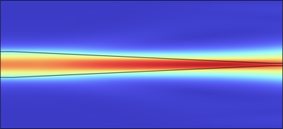
A tapered optical waveguide structure is used for matching two waveguides having different geometric cross sections and/or different material parameters. The tapered waveguide has one geometric cross section at the input plane and another cross section at the output plane. In between these planes, the core width changes linearly with the propagation distance.
This model demonstrates how to define a user-defined phase and wave vector for the Electromagnetic Waves, Beam Envelopes interface, when used with Perfectly Matched Layers (PMLs). The PMLs are used for absorbing the radiation that is not matching the port mode fields.
この model の例は, 通常次の製品を使用して構築されるこのタイプのアプリケーションを示しています.
ただし, これを完全に定義およびモデル化するには, 追加の製品が必要になる場合があります. さらに, この例は, 次の製品の組み合わせのコンポーネントを使用して定義およびモデル化することもできます.
アプリケーションのモデリングに必要な COMSOL® 製品の組み合わせは, 境界条件, 材料特性, フィジックスインターフェース, パーツライブラリなど, いくつかの要因によって異なります. 特定の機能が複数の製品に共通している場合もあります. お客様のモデリングニーズに適した製品の組み合わせを決定するために, 製品仕様一覧 を確認し, 無償のトライアルライセンスをご利用ください. COMSOL セールスおよびサポートチームでは, この件に関するご質問にお答えしています.