アプリケーションギャラリには電気, 構造, 音響, 流体, 熱および化学分野に関連する COMSOL Multiphysics® チュートリアルおよびデモアプリファイルが用意されています. これらの例はチュートリアルモデルまたはデモアプリファイルとそれに付随する手順をダウンロードすることにより独自のシミュレーション作業の開始点として使用できます.
クイック検索機能を使用して専門分野に関連するチュートリアルやアプリを検索します. MPHファイルをダウンロードするには, ログインするか, 有効な COMSOL ライセンスに関連付けられている COMSOL Access アカウントを作成します. ここで取り上げた例の多くは COMSOL Multiphysics® ソフトウェアに組み込まれ ファイルメニューから利用できるアプリケーションライブラリからもアクセスできることに注意してください.
This model and tutorial demonstrates the use of an Application Method to compute and plot the geometric Modulation Transfer Function (MTF) for the Petzval Lens. 詳細を見る
This model demonstrates how to simulate surface plasmon polaritons in a thin metal layer embedded in dielectric layers. It calculates the dispersion and propagation length of surface plasmon polaritons as a function of photon energy. 詳細を見る

This tutorial shows how to set up a multi-element objective lens. The chosen lens is the Double Gauss described in 'Modern Lens Design (2nd edition)', by W. Smith, 2005, pg 323. The tutorial demonstrates how to create a geometry sequence using the 'Spherical Lens 3D' part found in the ... 詳細を見る

This tutorial shows how to set up a multi-element objective lens. The chosen lens is a Petzval lens with field flattener described in 'Fundamental Optical Design', by M. Kidger, 2001, pg 192. The tutorial demonstrates how to include a geometric sequence using the 'Spherical General Lens ... 詳細を見る

This example demonstrates how to optimize the thickness of a microelectromechanical systems (MEMS) mirror coating material for maximum reflectivity. To reduce the simulation time, a Layered Impedance Boundary Condition is used to model the thin coating material on top of the metallic ... 詳細を見る
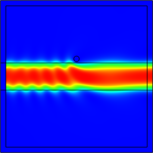
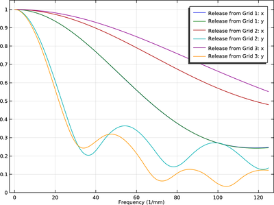
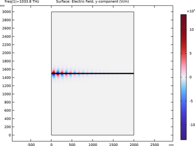
This model includes a dielectric slab waveguide with a small lossy metallic object nearby. The object causes light to be scattered, absorbed, and both reflected and transmitted along the waveguide. Learn more in this accompanying blog post: Modeling a Scatterer Near an Optical Waveguide 詳細を見る

Microlithography lenses are used to project the image of an integrated circuit onto a silicon substrate. This tutorial demonstrates how to create a 21-element fused silica lens which has a NA of 0.56 which is designed to be used at a wavelength of 248nm. The lens, which has a total ... 詳細を見る

This example shows how to perform parameter optimization on a lens system. The optimization is motivated by the replacement of one of the glasses in a prior optical prescription with a new glass having slightly different optical dispersion coefficients. The control parameters are the ... 詳細を見る

In its simplest form, an optical ring resonator consists of a straight waveguide and a ring waveguide. The waveguides are placed close to each other, making the light affect each between the two structures. If the propagation length around the ring is an integral number of wavelengths, ... 詳細を見る

This model demonstrates how to use topology optimization with milling constraints to design a metalens that focuses a single wavelength to a point. This involves transferring the optimized results to another component so the result can be verified using an explicit geometry ... 詳細を見る