アプリケーションギャラリには電気, 構造, 音響, 流体, 熱および化学分野に関連する COMSOL Multiphysics® チュートリアルおよびデモアプリファイルが用意されています. これらの例はチュートリアルモデルまたはデモアプリファイルとそれに付随する手順をダウンロードすることにより独自のシミュレーション作業の開始点として使用できます.
クイック検索機能を使用して専門分野に関連するチュートリアルやアプリを検索します. MPHファイルをダウンロードするには, ログインするか, 有効な COMSOL ライセンスに関連付けられている COMSOL Access アカウントを作成します. ここで取り上げた例の多くは COMSOL Multiphysics® ソフトウェアに組み込まれ ファイルメニューから利用できるアプリケーションライブラリからもアクセスできることに注意してください.

This tutorial demonstrates the use of the density-gradient formulation to include the effect of quantum confinement in the device physics simulation of a silicon inversion layer. This formulation requires only a moderate increase of computational resources as compared to the conventional ... 詳細を見る
This tutorial analyzes the DC characteristics of an InSb p-Channel FET, using the density-gradient theory to add the effect of quantum confinement to the conventional drift-diffusion formulation, without a large increase of computational resources. The confinement effect is applied both ... 詳細を見る

This model shows how to set up a 3D simulation of a n-p-n bipolar transistor. It is a 3D version of the device shown in the Bipolar Transistor model, and demonstrates how to extend semiconductor modeling into 3D using COMSOL Multiphysics. As in the 2D version of this model, the device ... 詳細を見る
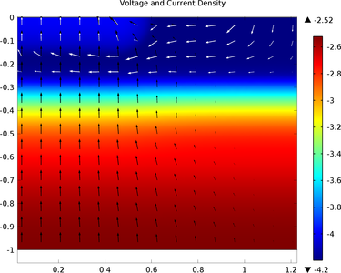
This benchmark example builds two models of a cross-bridge Kelvin resistor used for extracting the specific contact resistivity. The first model simulates the system in 3D, using the contact resistance feature built in the Semiconductor interface. The other model is a 2D approximation of ... 詳細を見る

In this second half of a two-part example, a 3D model of a trench-gate IGBT is built by extruding the 2D model from the first half. Unlike the 2D model, now it is possible to arrange the alternating n+ and p+ emitters along the direction of extrusion as in the real device. This more ... 詳細を見る
This model shows how to set up a simple Bipolar Transistor model. The output current-voltage characteristics in the common-emitter configuration are computed and the common-emitter current gain is determined. 詳細を見る

このチュートリアルでは, PIN ダイオードの定常応答とパルス応答の過渡解析をそれぞれ行います. 放射線の影響は, デバイス内で空間的に均一な電子-正孔対の生成としてモデル化されます. 高線量率では, 生成された電荷の分離により内部電場強度が減少し, 過剰キャリアが長期間蓄積されます. この現象の定量的な予測は, 解析解を得ることができないため, 数値シミュレーションによってのみ可能です. 高い逆バイアス, 電場依存移動度, および時間依存の解析において収束を達成するためのいくつかの手法を示します. 計算されたキャリア濃度と電場分布は, 参考文献とよく一致しています. 詳細を見る

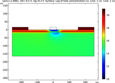
This model calculates the DC characteristics of a simple MOSFET. The drain current versus gate voltage characteristics are first computed in order to determine the threshold voltage for the device. Then the drain current vs drain voltage characteristics are computed for several gate ... 詳細を見る

This benchmark model simulates a GaAs nanowire using the self-consistent Schrödinger-Poisson theory to compute the electron density and the confining potential profiles. The predefined Schrödinger-Poisson multiphysics coupling feature is combined with the dedicated Schrödinger-Poisson ... 詳細を見る
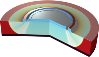
This model shows how to model the avalanche breakdown due to the impact ionization in a Silicon Carbide diode. The current-voltage (I-V) characteristics of the device are presented as well as the electric field distribution plot. Furthermore, the carrier generation term has been computed ... 詳細を見る