
Juan C. Cervantes-Gonzalez, Intel Guadalajara Design Center, Mexico
As the demand grows for faster electronic devices in smaller packages, we need to develop optimized high-speed interconnects, which transfer the signal between components in electronic devices. Found in printed circuit boards (PCB), this integral design element in electronics packaging carries signals laterally and through the depth of PCBs, traversing many layers of metal and dielectric material. To satisfy these growing technology demands, interconnects must be designed smaller, more closely packed, and able to operate at higher frequencies.
To reduce the number of prototypes required to test new interconnect designs, engineers at the Intel Guadalajara Design Center developed an efficient computational design optimization method, combining full-wave electromagnetic simulation in COMSOL Multiphysics® software with a space-mapping (SM) algorithm implemented in MATLAB® software. Through their approach, an interconnect design can be quickly optimized, streamlining the design cycle and time to market of the latest high-speed interconnect technology.
Suggested Stories
Express Delivery: Simulation App Speeds Up Electric Truck Battery Design
Volvo Trucks is using a simulation app to help optimize electric truck batteries. The app can be used to help produce ...
Illuminating Complex Material Behavior with Multiphysics Simulation
At Canadian Nuclear Laboratories, multiphysics simulation is used to gain insight into the behavior of nuclear fuel ...
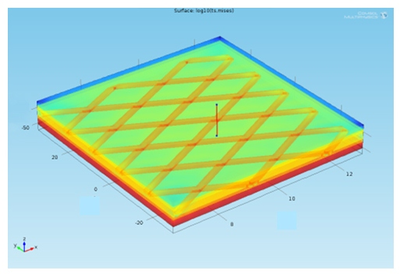
Boeing Simulates Thermal Expansion in Composites with Expanded Metal Foil for Lightning Protection of Aircraft Structures
Carbon fiber composites are used extensively throughout the body of modern aircraft, such as the Boeing 787 ...

Modeling Optimizes a Piezoelectric Energy Harvester Used in Car Tires
Siemens is a technology company working with electronics and electrical engineering in industry, energy, and ...


