
P. Woytowitz
Lam Research Corporation, CA, USA
With technological advancements accelerating so rapidly, more powerful computer chips are needed to meet the high demands of fast-growing industries. Lam Research Corporation manufactures semiconductor devices and equipment used to deposit, etch, and clean material layers laid onto wafers during semiconductor processing. With processes as precise as chemical vapor deposition (CVD), temperature fluctuations and thermal cycling can lead to defects in the deposition, selective removal, and patterning that are central to the manufacturing process.
Peter Woytowitz, director of engineering at Lam, has used COMSOL Multiphysics to understand how defects happen during manufacturing, and how wafer deformations correlate to overlay errors and misalignments. His team has designed a heating system for more uniform temperature control and simulated buckling in the temporary structures used for creating high-aspect ratio features. Using their results, they have been able to optimize their tool's performance, precisely match the degree of wafer displacement to overlay errors, and accurately predict buckling.
Suggested Stories
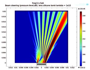
Optimizing Ultrasound Piezo-disk Transducers
Esaote S.p.A. produces medical diagnostic systems, including the manufacturing and sales of ultrasound imaging ...
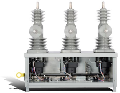
How Reclosers Ensure a Steady Supply of Power: It’s All in the Magnet
When a tree branch touches overhead cables and causes a momentary short circuit, your lights may flicker. A device ...
マルチフィジックスモデリングを通してブリルアンオプトメカニカルインタラクションを理解する
Campinas 大学とCorning の研究者は, 光弾性と移動境界効果がどのように連携して導波ガイド, 光ファイバー, その他のナノフォトニック構造におけるブリルアン散乱を増強(または抑制)させるかを見たいと考えていました. ...
Keynote: Simulation of MEMS Sensors at Bosch
In this keynote talk at the COMSOL Conference 2025 Amsterdam, Daniel Maier of Bosch discusses MEMS sensors and the ...


