
Besi Improved Memory Chip Manufacturing with Multiphysics Simulation
Stefan Behler, Besi, Switzerland
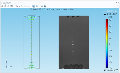
As memory chips become smaller and smaller, designers must ensure that the chips stay intact during the manufacturing process. Besi develops equipment and assembly processes for substrate and wafer packaging production in markets such as consumer electronics, automotive, industrial, and solar energy. Stefan Behler, a senior expert process engineer, used multiphysics simulation to explore and optimize a new way of peeling off the tape on a memory chip that results in less deformation of the dies. This new method is now used by semiconductor packaging factories all over the world.
Suggested Stories
ABBの電磁流量計デジタルツインがパフォーマンスを向上
ABBは仮想環境で実際の流量計を模擬するために電磁流量計のデジタルツインを構築しました. デジタルツインはマルチフィジックスモデリングに基づいてABBが流量計の設計を改善し, フィールド条件下でのデバイス性能を予測することを可能にします.
ライフサイエンス企業, CAE 専任部門の設立によりバイオ医薬品の研究開発を加速
バイオ医薬品は, 複雑な分子構造, 特殊な製造プロセス, そして業界に対する規制要件のために, 開発に多額の費用がかかります. ライフサイエンス企業である Sartorius 社は, マルチフィジックスシミュレーションを活用しています.
Floating on Sound Waves with Acoustic Levitation
As part of an industry that saves lives on a regular basis, pharmaceutical companies are in need of systems that can ...
Multiphysics Analysis Helps Preserve the Past
Jos van Schijndel is the founder of Netherlands-based consulting firm CompuToolAble and assistant professor at ...


