
Besi Improved Memory Chip Manufacturing with Multiphysics Simulation
Stefan Behler, Besi, Switzerland
As memory chips become smaller and smaller, designers must ensure that the chips stay intact during the manufacturing process. Besi develops equipment and assembly processes for substrate and wafer packaging production in markets such as consumer electronics, automotive, industrial, and solar energy. Stefan Behler, a senior expert process engineer, used multiphysics simulation to explore and optimize a new way of peeling off the tape on a memory chip that results in less deformation of the dies. This new method is now used by semiconductor packaging factories all over the world.
Suggested Stories
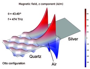
Surface Plasmon Resonance
Surface Plasmon Resonance (SPR) is created by surface plasmons, coherent electron oscillations existing between any ...
Numerical Simulation-Based Topology Optimization Leads to Better Cooling of Electronic Components in Toyota Hybrid Vehicles
The Toyota Research Institute in Ann Arbor drives cutting-edge research in energy efficiency, mobility infrastructure, ...
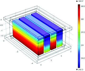
Simulation Helps Improve Atmosphere Revitalization Systems for Manned Spacecraft
To ensure astronaut safety on space missions, it is necessary to routinely revitalize the atmosphere in manned ...
核融合の未来へのタイムラインを短縮
General Fusion 社は, マルチフィジックスシミュレーションを活用し, 核融合実証機の設計と最適化に成功しました. 現在, この装置は定期的にプラズマを生成しています.


