
Besi Improved Memory Chip Manufacturing with Multiphysics Simulation
Stefan Behler, Besi, Switzerland
As memory chips become smaller and smaller, designers must ensure that the chips stay intact during the manufacturing process. Besi develops equipment and assembly processes for substrate and wafer packaging production in markets such as consumer electronics, automotive, industrial, and solar energy. Stefan Behler, a senior expert process engineer, used multiphysics simulation to explore and optimize a new way of peeling off the tape on a memory chip that results in less deformation of the dies. This new method is now used by semiconductor packaging factories all over the world.
Suggested Stories
Keynote: Optimum Electromagnetic and Thermal Design of DC-Link Capacitors
Inverters change the DC produced by an electric vehicle's battery into the AC needed to drive its motors. Inside these ...
ITW はマルチフィジックスシミュレーションを使用して賢い電子レンジオーブンを設計します
固体熱伝導加熱を備えた「スマートオーブン」を設計するために, Illinois Tool Works (ITW) 食品機器グループのエンジニアはマルチフィジックスシミュレーションと特殊なアプリケーションに目を向けました. ...
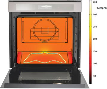
Simulation Turns Up the Heat and Energy Efficiency at Whirlpool Corporation
Engineers working on a joint research project between Whirlpool Corporation and the European initiative GREENKITCHEN ...
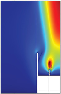
Multiphysics Analysis of a Burning Candle
Using COMSOL Multiphysics, AltaSim Technologies were able to predict the temperature distribution and flow pattern of ...


