
Tokyo Electron Pushes the Limits of Chip Density with Simulation
Derek Bassett and Michael Carcasi
Tokyo Electron America
Austin, TX
Chip manufacturers have been adhering to Moore’s law, a law stating that the number of transistors that can be economically placed on an integrated circuit doubles every year, since 1965. As the number of transistors increases, however, the process of manufacturing integrated circuit, called photolithography, becomes more difficult. Each device requires approximately 200 cleaning and photolithography steps and any failures in this process can cost millions.
Tokyo Electron America (TEL), a producer of manufacturing tools vital to the processing of integrated circuits, used simulation to understand a type of failure called pattern collapse. Pattern collapse occurs when cleaning fluid between two features evaporates and the changing surface tension occurring during the evaporation causes the features to bend. Ideally, those features return to their normal shape, but sometimes they are permanently deformed.
Using COMSOL Multiphysics, researchers at TEL created a 2D structural mechanics model based on a series of steady-state calculations with the surface tension forces as boundary conditions. They compared those results with experimental data from literature and found that the model accurately predicted the critical aspect ratio for collapse.
Suggested Stories
シミュレーションアプリケーションが電気自動車モーターの開発を合理化
Volkswagen Kassel はローターラミネーションの強度を評価するシミュレーションアプリケーションを構築および配布することにより, 電気モーターの設計プロセスを加速します. ...
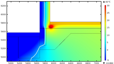
Using Multiphysics Simulation to Prevent Building Damage
In addition to surviving normal winters, a strong building must be able to survive the worst winters expected in a 50 ...
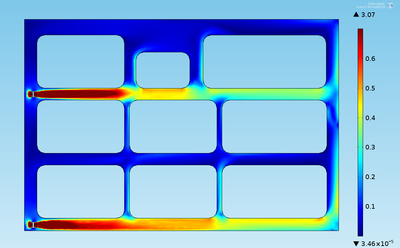
Battling Corrosion in Nuclear Waste Storage Facilities
Nuclear sites in Italy are being decommissioned, leaving questions about how to safely manage and store radioactive ...
高速通信用のワイヤレステストシステムとアンテナの最適化
ワイヤレステストソリューションのパイオニアであるBluetestは, ワイヤレスデバイスと広帯域アンテナのパフォーマンスを測定するために使用される残響システムを設計しています. 彼らはRFシミュレーションを使用して, 設計, 製造, ...


