Predictive Simulations of Warpage Phenomena on Arbitrarily Patterned Silicon Wafers
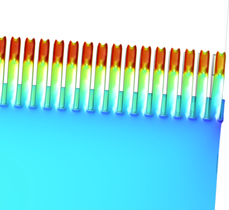
In this simulation, we aim to comprehend the origin and mechanism of the warpage phenomenon in patterned silicon wafers, which are key components in the field of microelectronics. This issue can become more pronounced in the presence of high global density of the patterns and can lead to wafer handling problems resulting in the blocking of the production process.In our study, the device under investigation exhibits a highly directional pattern of aligned trenches spanning the entire surface of the silicon wafer. The simulation encompasses three primary process steps: gate oxide growth, trench filling with doped polysilicon, and implants annealing at 1100°C. The ongoing simulation process utilizes the Structural Mechanics Module in the steady state, aiming to directly incorporate the intrinsic stresses generated by the process steps instead of employing thermal expansion phenomena. The input values of the intrinsic stresses have been experimentally measured in the laboratories of ST Microelectronics, a collaborating company in this PhD project. By incorporating the intrinsic stresses from the thermal cycles experienced during each step, it becomes possible to perform static simulations without relying directly on thermal expansions. Given the nanoscale dimensions and the presence of thousands of aligned trenches, we have chosen to simulate a three-dimensional unit cell (figure 1). Stresses resulting in the warpage phenomenon will be extrapolated from this unit cell and utilized to simulate the deformation of the entire wafer during the final phase of the project. We varied primarily the dimensional parameters, including length and quantity of the trench, or shape of the orthogonal section (square, rectangular, or circular), to evaluate their impact on the final results. We compared the results with experimental data on bow and deformation measured on real wafers, to assess the efficacy of the simulation and to fine tune several simulation parameters. As a result, the first phase of the project was successfully concluded. In the second phase, we target to simulate the remaining two process steps, which are inherently more complex than the initial one. Additionally, we will strive to address a multiphysics problem by incorporating the heating effects of current flow using the AC/DC Module. The final phase will involve employing the data extrapolated from the unit cell to simulate a quarter-wafer, which, due to symmetry, provides an accurate representation of the entire geometry. The issue of warpage, once considered of secondary importance, now poses significant challenges in current microelectronics, which is one of the most critical and rapidly evolving sectors of our society. Although the COMSOL Multiphysics® simulation in this project involves structural and physical simplifications, it serves as a pivotal initial step towards solving the warpage problem.
ダウンロード
- Sabatini_4441_poster.pdf - 3.92MB