イベント開始: 08:00 – 20:00
検索
予定されているイベント
イベントをロード中
3月 3
| 8:00 CET
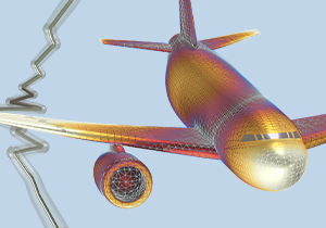
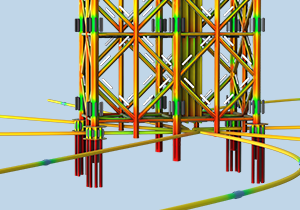
Modeling for Aerospace Engineering with COMSOL Multiphysics®
COMSOL
ウェビナー
オンライン
3月 3–6
| 11:00 EST
Introduction to COMSOL Multiphysics®
COMSOL
トレーニングコース
オンライン

3月 3
| 14:00 EST
Editing, Repairing, and Combining Imported STL Files with CAD
COMSOL
ウェビナー
オンライン
3月 10
| 9:00 CET
GPU Acceleration in COMSOL®
COMSOL
ウェビナー
オンライン

3月 10
| 10:00 GMT
Time-Optimal Control with COMSOL Multiphysics® in 18 Minutes
COMSOL
ウェビナー
オンライン

3月 10–13
| 11:00 EDT
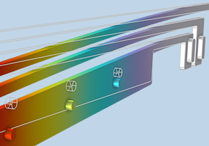
CFD Modeling in COMSOL Multiphysics®
COMSOL
トレーニングコース
オンライン
3月 12
| 14:00 EDT
Phased-Array Antenna Modeling: Techniques to Optimize RF Design
Machine/Electronic Design
ウェビナー
オンライン

3月 15–19
| 10:00 CDT
AMPP
COMSOL
Exhibition
Houston
3月 17
| 9:00 CET
CFD Modeling with COMSOL® in 18 Minutes
COMSOL
ウェビナー
オンライン
3月 17–19
| 9:00 EDT
Optical Fiber Communications Exhibition
COMSOL
Exhibition
Los Angeles

3月 17
| 11:00 EDT
Modeling Gyroscopes and Accelerometers in COMSOL Multiphysics®
COMSOL
ウェビナー
オンライン
3月 23–26
| 9:00 EDT
International Battery Seminar
COMSOL
Exhibition
Orlando
3月 24–27
| 11:00 EDT
AC/DC Modeling in COMSOL Multiphysics®
COMSOL
トレーニングコース
オンライン
3月 25
| 10:00 GMT
Solving Large Models in COMSOL Multiphysics®
COMSOL
ウェビナー
オンライン

3月 26
| 11:00 EDT
Photo-Thermo-Optical Effects in Metasurfaces: From Optical to Thermochemical Devices
Photonics Spectra
ウェビナー
オンライン

3月 26
| 11:00 EDT
COMSOL Day: Electric Power
COMSOL
COMSOL デー
オンライン

4月 14
| 8:00 CEST
Modeling Granular Flow in COMSOL®
COMSOL
ウェビナー
オンライン
4月 14–17
| 11:00 EDT
Introduction to COMSOL Multiphysics®
COMSOL
トレーニングコース
オンライン
4月 21
| 8:00 CEST
Simulation Apps & Digital Twins for the Renewable Energy Industry
COMSOL
ウェビナー
オンライン
4月 21–24
| 11:00 EDT
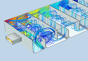
Heat Transfer Modeling in COMSOL Multiphysics®
COMSOL
トレーニングコース
オンライン
4月 28–29
| 9:00 EDT
Introduction to COMSOL Multiphysics®
COMSOL
トレーニングコース
Burlington
5月 5–8
| 11:00 EDT
Acoustics Modeling in COMSOL Multiphysics®
COMSOL
トレーニングコース
オンライン

5月 8
| 12:00 PDT
COMSOL Simulation Summit: Santa Clara
COMSOL
Summit
Santa Clara
5月 12
| 8:00 CEST
Equation-Based Modeling with COMSOL®
COMSOL
ウェビナー
オンライン
5月 19
| 8:00 CEST
Preparing CAD for Analysis with COMSOL®
COMSOL
ウェビナー
オンライン
5月 19–22
| 11:00 EDT
Introduction to COMSOL Multiphysics®
COMSOL
トレーニングコース
オンライン
6月 9
| 8:00 CEST
Modeling Electric Motors & Generators
COMSOL
ウェビナー
オンライン
6月 23
| 8:00 CEST
CFD Modeling with COMSOL® in 18 Minutes
COMSOL
ウェビナー
オンライン
6月 23–26
| 11:00 EDT
Introduction to COMSOL Multiphysics®
COMSOL
トレーニングコース
オンライン
29 中の 8 を表示
29 中の 29 を表示
オンデマンドウェビナー

Modeling Rotordynamics with COMSOL Multiphysics®
ウェビナー
Feb 26

Modeling Nonlinear Photonics in Dielectric Resonant Metasurfaces Using COMSOL®
ウェビナー
Feb 18
Modeling and Simulation of MEMS Devices
ウェビナー
Feb 04
Modeling Photonic Crystals in COMSOL Multiphysics
ウェビナー
Jan 29

Modeling Emerging Battery Technologies with COMSOL Multiphysics®
ウェビナー
Jan 28
The Basics of COMSOL Multiphysics® in 18 Minutes
ウェビナー
Jan 27
Shape and Topology Optimization with COMSOL Multiphysics®
ウェビナー
Jan 22
Automotive Acoustics Analysis Using COMSOL Multiphysics
ウェビナー
Jan 21

Polymer Flow Modeling
ウェビナー
Jan 13
Parameter Estimation for Nonlinear Materials
ウェビナー
Dec 11

Introducing COMSOL Multiphysics® Version 6.4
ウェビナー
Dec 10
Multiphysics Simulation of Power Transformers
ウェビナー
Dec 09
Multiphysics Simulation for Vehicle Electrification
ウェビナー
Dec 02
Optimising Manufacturing Processes Through Simulation
ウェビナー
Nov 26
Designing Efficient Electric Motors with COMSOL Multiphysics
ウェビナー
Nov 26

Efficient Battery Modeling with Surrogate Models
ウェビナー
Nov 19

Automating Your Modeling Workflow in COMSOL Multiphysics®
ウェビナー
Nov 18
The Basics of COMSOL Multiphysics® in 18 Minutes
ウェビナー
Nov 11

Modeling Pipe Flow & Heat in COMSOL Multiphysics®
ウェビナー
Nov 06
Modeling Gyroscopes and Accelerometers in COMSOL Multiphysics®
ウェビナー
Oct 30
Modeling and Simulation for Electric Motor Design
ウェビナー
Oct 15
Simulating Electrical Power Systems for the Grid
ウェビナー
Oct 14
Unravelling Chemomechanical Effects in Lithium-Ion Batteries
ウェビナー
Oct 09
Modeling Next-Generation Battery Technologies with COMSOL Multiphysics®
ウェビナー
Oct 06
Modeling Emerging Battery Technologies with COMSOL Multiphysics®
ウェビナー
Sep 25
Modeling and Simulation of MEMS Devices
ウェビナー
Sep 23
Modeling Reaction Kinetics and Pharmacokinetics with COMSOL Multiphysics®
ウェビナー
Sep 11
Modeling Ultrasound for Biomedical Applications
ウェビナー
Sep 09

Optimization of Thermal Management Systems
ウェビナー
Sep 03

Prediction of Electromagnetic Signatures of Naval Vessels with COMSOL Multiphysics
ウェビナー
Aug 28

Modeling Room Acoustics in COMSOL Multiphysics®
ウェビナー
Aug 19
Modeling and Simulation for Electric Motor Design
ウェビナー
Aug 14

Moisture Transport Modeling in COMSOL Multiphysics®
ウェビナー
Aug 07
Modeling Hydrogen Fuel Cells and Electrolyzers
ウェビナー
Aug 06
The Basics of COMSOL Multiphysics® in 18 Minutes
ウェビナー
Aug 05
Modeling Acoustic Metamaterials in COMSOL Multiphysics
ウェビナー
Jul 31

Fatigue and Durability Analysis Using COMSOL Multiphysics®
ウェビナー
Jul 24

Biomedical Modeling with COMSOL Multiphysics
ウェビナー
Jul 17
Understanding Liquid Metal Transport in Magnetic Fields — Simulating Magnetohydrodynamic Duct Flow
ウェビナー
Jul 11
Modeling Electric Motors and Drivetrains
ウェビナー
Jul 10

Memristor Modeling with COMSOL Multiphysics®
ウェビナー
Jul 02
Underwater Acoustics
ウェビナー
Jun 12
Optimization in Structural Mechanics
ウェビナー
Jun 12
Hydrogen Technology Innovation with Simulation
ウェビナー
Jun 12
Modeling Hydrogen Fuel Cells and Electrolyzers
ウェビナー
Jun 12
Modeling Chemical Reactions and Reacting Flows Using COMSOL Multiphysics®
ウェビナー
Jun 05
Introduction to Multibody Dynamics Modeling with COMSOL Multiphysics
ウェビナー
May 28
Automotive Acoustics Analysis Using COMSOL Multiphysics®
ウェビナー
May 27

Improving Thermal Management of Batteries with COMSOL Multiphysics®
ウェビナー
May 09

The Basics of COMSOL Multiphysics® in 18 Minutes
ウェビナー
Apr 15

Wave & Ray Optics Modeling with COMSOL®
ウェビナー
Apr 09

Optimization in RF and Wave Optics
ウェビナー
Apr 09

Multiphysics Simulation in Semiconductor Packaging
ウェビナー
Apr 03
Acoustics in Electronics Webinar Series, Part 1: Loudspeakers
ウェビナー
Mar 25
Simulating Electrical Power Systems for the Grid
ウェビナー
Mar 20
Multiphysics Modeling of Electronic Components
ウェビナー
Mar 20
Improving Thermal Management of Batteries with COMSOL Multiphysics®
ウェビナー
Mar 18

Modeling Chemical Reactions and Reacting Flows Using COMSOL Multiphysics®
ウェビナー
Mar 06
58 中の 6 を表示
58 中の 58 を表示
- 製品情報
- 製品概要
- 製品仕様一覧
- ソフトウェアライセンスの種類
- 動作環境
- リリース履歴
- 会社情報
- COMSOLについて
- 採用情報
- プレスリリース
- お問い合わせ
- |
- プライバシーポリシー
- |
- 商標について
- |
- Cookie Settings
- © 2026 by COMSOL. All rights reserved