Webinar Series Multiphysics Modeling of Semiconductors
Multiphysics Modeling of Semiconductors
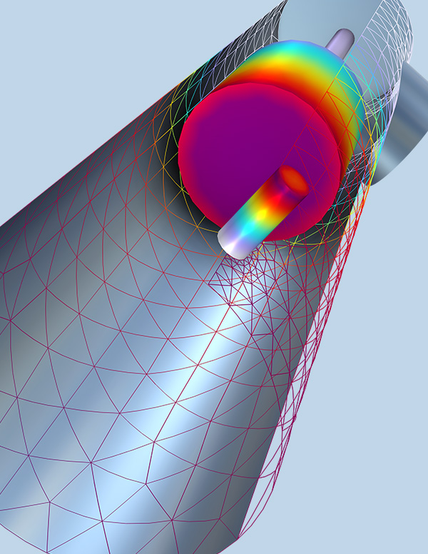
As semiconductor devices become more advanced and design constraints become more demanding, multiphysics modeling has become an essential tool for design, optimization, and verification. This webinar series will demonstrate how COMSOL Multiphysics® can be used to simulate semiconductor applications, with a focus on three key areas:
- Semiconductor packaging & testing
- Semiconductor device physics
- Semiconductor surface processing
Through live demonstrations, and application-focused examples, this series will showcase how multiphysics simulations can be used to simulate semiconductor devices at the fundamental physics level, model manufacturing processes, and evaluate interactions between semiconductor materials and other physical phenomena.
We will share practical insights and modeling approaches for developing next-generation semiconductor technologies using COMSOL Multiphysics®.
Register for one or more webinars using the links below.
Part 1: Packaging & Testing | July 21

See how multiphysics simulation can be used to analyze and optimize semiconductor packaging designs, improving thermal performance, reliability, and signal integrity in advanced electronic devices.
Part 2: Device Physics | July 28

Learn how semiconductor device simulation can be used to analyze carrier transport, quantum effects, and multiphysics interactions in advanced electronic and optoelectronic devices.
Part 3: Surface Processing | August 4

Gain insight into predicting and optimizing plasma-assisted deposition and etching processes through coupled simulations of plasma physics, electromagnetics, fluid flow, heat transfer, and surface chemistry.