Simulation of the Frequency Response of a Mach-Zehnder Modulator Actuated by a PZT Chip
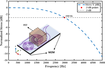
Integrating piezoelectric actuators onto photonic integrated circuits equips passive photonic components with active tunability and modulation capabilities [1]. Lead zirconate titanate (PZT) chips have been hybrid integrated onto microring resonators to demonstrate tunable external cavity lasers [2], as well as onto Mach-Zehnder interferometers to realize highly efficient phase modulation [3]. When electrically biased, the PZT chip induces mechanical deformation, which further introduces stress and strain to the underlying optical waveguide, altering its effective mode index via the stress-optic effect. While the modulation efficiency under static (DC) driving conditions has been numerically modeled [4] and been applied to control resonance splitting [5], systematic modeling of frequency response under alternating-current (AC) driving condition remains unexplored. In this work, we develop a 3D finite-element simulation model in COMSOL Multiphysics® to evaluate the electro-optic (EO) modulation bandwidth of a PZT-actuated photonic chip. Adopting the structural geometry from our prior experimental work [3], we establish a simplified 3D model comprising a top PZT actuator bonded to a SiO2/Ta2O5/SiO2 photonic platform. The PZT chip (TA0505D024W, Thorlabs®) is attached via a 150 μm-thick epoxy resin adhesive layer (EP31ND, Master Bond®), as shown in Fig. 1. Anisotropic piezoelectric and mechanical properties are assigned to each domain. We first perform a Stationary study with the help of the Solid Mechanics (solid) and Electrostatics (es) interfaces within the Structural Mechanics and AC/DC modules to analyze the static stress distribution on the photonic chip. Fig. 2 displays the structural deformation under a DC bias of 10 V. The induced in-plane stresses (Sx and Sy) along the cut-line [Fig. 3(a)] that passes through the waveguide layer is shown in Fig. 3(b). These results indicate that the transferred stress is highly spatially dependent, with the central region providing a relatively uniform biaxial stress in contrast to the sharp variations at the edges. To characterize the frequency response, we then conduct frequency domain study in the Structural Mechanics and AC/DC modules. A frequency sweep from 0 to 5000 Hz is performed at a fixed 10 V voltage amplitude. By evaluating the y-stress at the waveguide layer beneath the PZT center point, the frequency response is obtained in Fig. 4, revealing the 3 dB bandwidth is 2985 Hz. The simulated result aligns well with our experimental measurements. The EO bandwidth is primarily limited to the mechanical damping from the epoxy layer [2]. The simulation framework provides a robust design methodology for modeling and optimizing integrated Mach-Zehnder modulators and microring resonators that are actuated by top-bonded PZT chips.