研究開発におけるマルチフィジックスシミュレーションの具体例
さまざまな業界のエンジニア, 研究者, 科学者がマルチフィジックスシミュレーションを使用して革新的な製品の設計とプロセスを研究および開発しています. COMSOL カンファレンスで発表したテクニカルペーパーやプレゼンテーションからインスピレーションを得てください. 以下の選択項目を参照するか, クイック検索ツールを使用して特定のプレゼンテーションを検索するか, アプリケーション領域でフィルタリングします.
COMSOL Conference 2024 論文集を見る
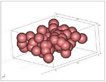
Finite Element analysis is used to model 2-D and 3-D paraelectric-dielectric composites (BaTiO3 spherical fillers randomly distributed in constant dielectric matrix). The effective dielectric response and tunability are studied under different filler sizes and different volume fractions. ... 詳細を見る

Microplasmas at atmospheric pressure are required in many applications, where treatments in normal ambient, with spatial resolution, are important. The interest on such miniaturized sources has increased due to the availability of a new generation of microwave sources based on high power ... 詳細を見る

The Microwave Electrothermal Thruster (MET) is a space electric propulsion device that uses an electromagnetic resonant cavity within which a free-floating plasma is ignited and sustained, heating a propellant gas that is that exhausted out of a gas-dynamic nozzle. For an empty cavity ... 詳細を見る

Magnetic fluids containing nano or submicron magnetic particles and their application in food, biological and pharmaceutical systems have recently attracted increasing attention. Magnetic particles can be collected efficiently in magnetizable matrices (e.g. iron wires) in high gradient ... 詳細を見る
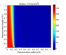
A mathematical model is developed for the stripping of CO2 from rich solvent. The rich solvent (aqueous NaOH) is used in CO2 absorption from natural gas through gas-liquid hollow fiber membrane contactor. The polyvinylidene fluoride (PVDF) hollow fiber membrane was fabricated via ... 詳細を見る
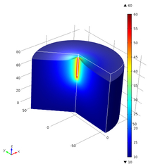
The authors are currently investigating the use of bulk high temperature superconductors as trapped field magnets (TFMs) in order to increase the electrical and magnetic loading of an axial gap, trapped flux-type superconducting electric machine. In electric machines, the use of ... 詳細を見る
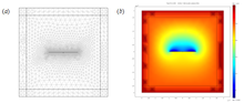
The maintenance plan or rush-to-repair of a subsea pipeline for oil transport may result in the shutdown of the line, in other words, may stop the flow of fluid. During the shutdown, the temperature of the oil tends to decrease continuously, and the heavy molecules tend to crystallize ... 詳細を見る
The idea of application as a hearing device based on a parasitoid fly, Ormia ochracea has been studied extensively recently. This paper addresses another possible application as an underwater directional sensor. In order to study the feasibility of the application, it is necessary to ... 詳細を見る
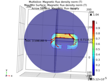
This report mainly discusses the implementation and results of a project proposal, “Modelling using Finite Element Methods”. The report is devoted to implementation, which is a model of an electromagnet. The software tool that is used to model the electromagnet is COMSOL Multiphysics®, a ... 詳細を見る
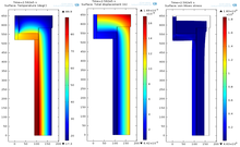
Energy piles, i.e. heat exchangers located within the foundation piles of buildings, are used for heating of cooling purposes. Although the absolute values of deformations and temperature gradients are low or moderate, the entire setting can be influenced by thermo-hydro-mechanical ... 詳細を見る