
Juan C. Cervantes-Gonzalez, Intel Guadalajara Design Center, Mexico
As the demand grows for faster electronic devices in smaller packages, we need to develop optimized high-speed interconnects, which transfer the signal between components in electronic devices. Found in printed circuit boards (PCB), this integral design element in electronics packaging carries signals laterally and through the depth of PCBs, traversing many layers of metal and dielectric material. To satisfy these growing technology demands, interconnects must be designed smaller, more closely packed, and able to operate at higher frequencies.
To reduce the number of prototypes required to test new interconnect designs, engineers at the Intel Guadalajara Design Center developed an efficient computational design optimization method, combining full-wave electromagnetic simulation in COMSOL Multiphysics® software with a space-mapping (SM) algorithm implemented in MATLAB® software. Through their approach, an interconnect design can be quickly optimized, streamlining the design cycle and time to market of the latest high-speed interconnect technology.
Suggested Stories
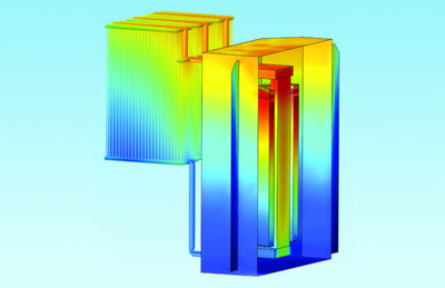
Simulation Enables the Next Generation of Power Transformers and Shunt Reactors
From power generation to its distribution to end users, power transformers and shunt reactors are used throughout the ...
Get an Inside Look at How Veryst Engineering Looks Inside Designs
Step into the material test lab at Veryst Engineering to see how they develop accurate material models for use in ...

6 シミュレーション主導のスピーカー開発例
バーチャルリアリティゲーム用のヘッドフォンから補聴器用の強力なトランスデューサーまで, マルチフィジックスシミュレーションがスピーカーの新製品や改良品の開発に活用されている6つの事例をご紹介します.
Express Delivery: Simulation App Speeds Up Electric Truck Battery Design
Volvo Trucks is using a simulation app to help optimize electric truck batteries. The app can be used to help produce ...


