
Juan C. Cervantes-Gonzalez, Intel Guadalajara Design Center, Mexico
As the demand grows for faster electronic devices in smaller packages, we need to develop optimized high-speed interconnects, which transfer the signal between components in electronic devices. Found in printed circuit boards (PCB), this integral design element in electronics packaging carries signals laterally and through the depth of PCBs, traversing many layers of metal and dielectric material. To satisfy these growing technology demands, interconnects must be designed smaller, more closely packed, and able to operate at higher frequencies.
To reduce the number of prototypes required to test new interconnect designs, engineers at the Intel Guadalajara Design Center developed an efficient computational design optimization method, combining full-wave electromagnetic simulation in COMSOL Multiphysics® software with a space-mapping (SM) algorithm implemented in MATLAB® software. Through their approach, an interconnect design can be quickly optimized, streamlining the design cycle and time to market of the latest high-speed interconnect technology.
Suggested Stories
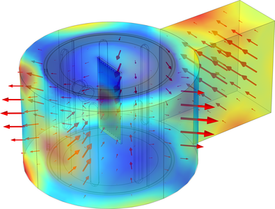
Developing a New Microreactor for Organic Synthesis Using Microwave Heating
The chemical reactions used to generate solvents and certain pharmaceuticals rely on organic synthesis, a process of ...
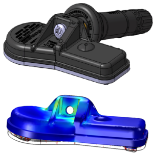
Optimizing Built-in Tire Pressure Monitoring Sensors
Built-in tire pressure sensors need to be able to withstand the wear and tear of working within a car’s tire rim. ...
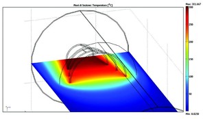
Around the Clock Solar Power
Italian utility ENEL and the Italian National Agency for New Technologies joined together to develop a new kind of ...

Engineering Great Sound: Predicting Loudspeaker Thermal Performance at Amazon
Amazon's audio technology team develops a variety of audio systems for its customers, relying on multiphysics ...


