Besi Improved Memory Chip Manufacturing with Multiphysics Simulation
Stefan Behler, Besi, Switzerland
As memory chips become smaller and smaller, designers must ensure that the chips stay intact during the manufacturing process. Besi develops equipment and assembly processes for substrate and wafer packaging production in markets such as consumer electronics, automotive, industrial, and solar energy. Stefan Behler, a senior expert process engineer, used multiphysics simulation to explore and optimize a new way of peeling off the tape on a memory chip that results in less deformation of the dies. This new method is now used by semiconductor packaging factories all over the world.
Suggested Stories
Engineering Perfect Puffed Snacks
The production of puffed rice, like many other types of food, is incredibly complicated and involves multiple ...
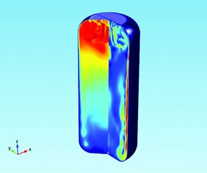
Modeling Helps Improve Safety in the Production of Teflon
BAM German Federal Institute for Materials Research & Testing in Berlin promotes industrial development by ...
がん個別化医療を支援するシミュレーションアプリが登場
バジリカータ大学のスピンオフ企業である iBMB は, 乳がんの腫瘍の進行を腫瘍内科医がより正確にモニタリング・評価できるよう支援するシミュレーションアプリを開発しました. このアプリは, 臨床現場への導入が可能な段階にあります.
Multiphysics Analysis Helps Preserve the Past
Jos van Schijndel is the founder of Netherlands-based consulting firm CompuToolAble and assistant professor at ...