
Besi Improved Memory Chip Manufacturing with Multiphysics Simulation
Stefan Behler, Besi, Switzerland
As memory chips become smaller and smaller, designers must ensure that the chips stay intact during the manufacturing process. Besi develops equipment and assembly processes for substrate and wafer packaging production in markets such as consumer electronics, automotive, industrial, and solar energy. Stefan Behler, a senior expert process engineer, used multiphysics simulation to explore and optimize a new way of peeling off the tape on a memory chip that results in less deformation of the dies. This new method is now used by semiconductor packaging factories all over the world.
Suggested Stories
Simulation Apps Bring STEM to Life
While covering the required fundamental material in undergraduate academic programs is the top priority, students ...
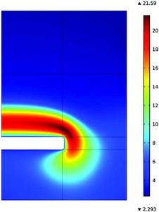
Capacitively Coupled Plasma Analysis
AltaSim Technologies provides engineering consulting services involving advanced multiphysics modeling such as ...
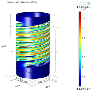
Meeting High-Speed Communications Energy Demands Through Simulation
The information and communication technology industry needs new energy-efficient devices that can keep up with the ...
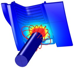
Switching Made Easy
Modern cars offer a wide range of complex functionality that comes with several design challenges. This story ...


