
Besi Improved Memory Chip Manufacturing with Multiphysics Simulation
Stefan Behler, Besi, Switzerland
As memory chips become smaller and smaller, designers must ensure that the chips stay intact during the manufacturing process. Besi develops equipment and assembly processes for substrate and wafer packaging production in markets such as consumer electronics, automotive, industrial, and solar energy. Stefan Behler, a senior expert process engineer, used multiphysics simulation to explore and optimize a new way of peeling off the tape on a memory chip that results in less deformation of the dies. This new method is now used by semiconductor packaging factories all over the world.
Suggested Stories
砂に蓄えた太陽エネルギーで建物を暖める
Polar Night Energy は, 熱モデリングを使用して, 42トンの砂を動力源とする蓄熱および配電システムの設計を最適化しました. このプロジェクトは, ...

Multiphysics Simulations Enable Development of Fast, Cheap MEMS-Based Bacteria Detector
Professor Mark Reed and his team at Yale University are using COMSOL Multiphysics to develop a MEMS-based solution for ...
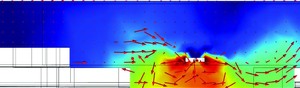
Restoration of Lake Water Environments
Human activity steals oxygen from natural water sources such as lakes and this oxygen-deficient water often contains ...
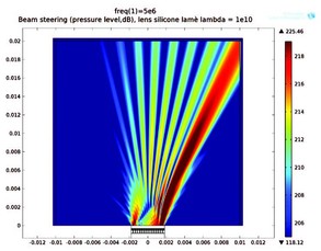
Optimizing Ultrasound Piezo-disk Transducers
Esaote S.p.A. produces medical diagnostic systems, including the manufacturing and sales of ultrasound imaging ...


