アプリケーションギャラリには電気, 構造, 音響, 流体, 熱および化学分野に関連する COMSOL Multiphysics® チュートリアルおよびデモアプリファイルが用意されています. これらの例はチュートリアルモデルまたはデモアプリファイルとそれに付随する手順をダウンロードすることにより独自のシミュレーション作業の開始点として使用できます.
クイック検索機能を使用して専門分野に関連するチュートリアルやアプリを検索します. MPHファイルをダウンロードするには, ログインするか, 有効な COMSOL ライセンスに関連付けられている COMSOL Access アカウントを作成します. ここで取り上げた例の多くは COMSOL Multiphysics® ソフトウェアに組み込まれ ファイルメニューから利用できるアプリケーションライブラリからもアクセスできることに注意してください.

The homogenized material properties of a composite are computed based on the temperature-dependent properties of matrix and fiber. The homogenized parameters are compared to the analytical values derived from the rule of mixtures. This is an extension of model https://www.comsol.com ... 詳細を見る

Beam theories are well-developed for slender structures with homogeneous materials and isotropic cross-sections. The traditional beam theories do no apply to beams made of different materials in the cross-section. Therefore, a homogenization-based numerical model is needed to compute ... 詳細を見る
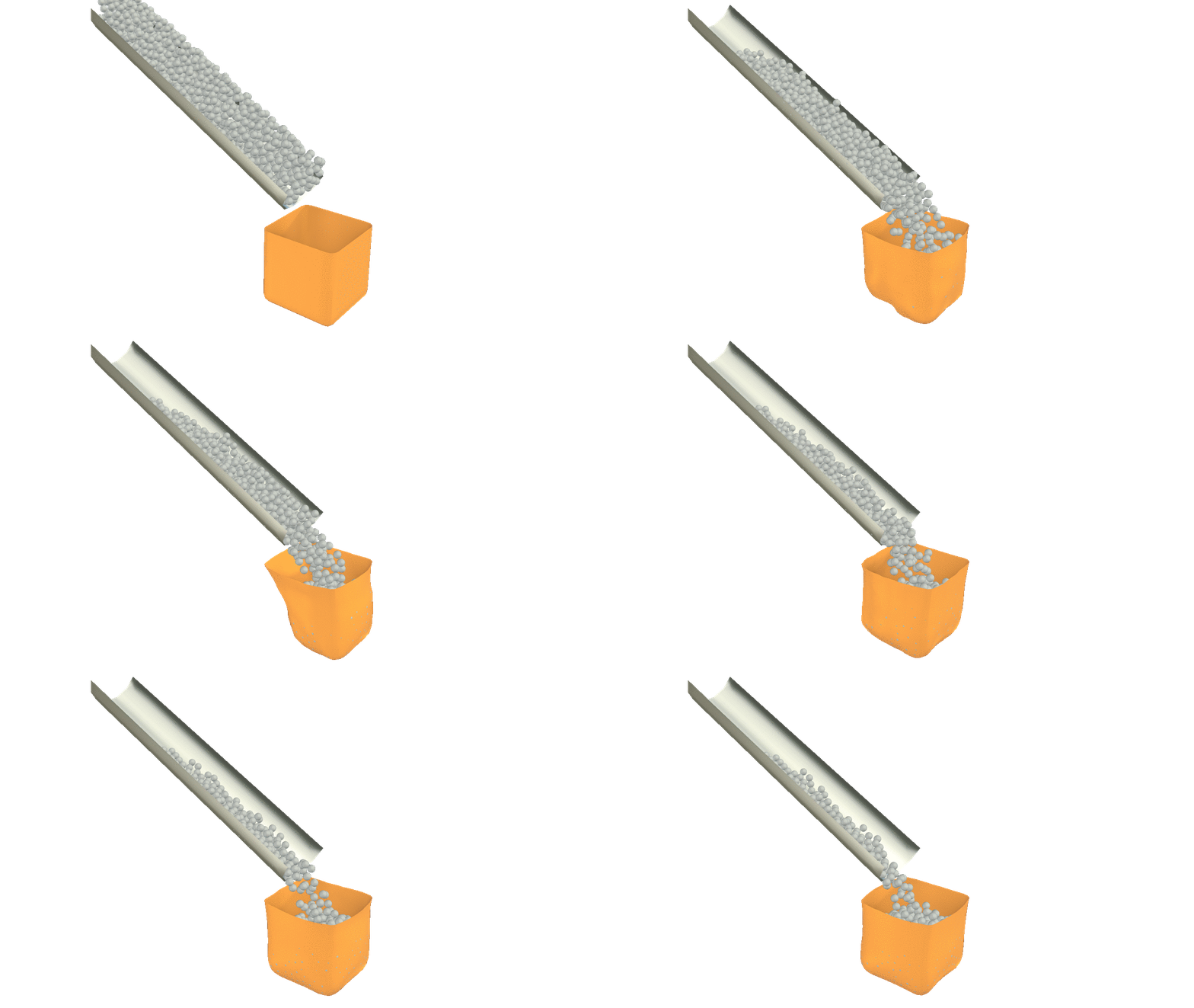
This model uses the Granular Flow and Membrane interfaces to simulate the packing of spherical grains in a flexible container, a procedure often found in the processing industry. In this example, grains are packed into a cubic container constructed of a thin polymer fabric. Two packing ... 詳細を見る

In semiconductor manufacturing, vacuum chucks are used to rapidly and contamination-free adsorb and secure wafers before processes such as transfer, lithography, and inspection. Traditional empirical design makes it difficult to quantify the effects of groove shape, size, distribution, ... 詳細を見る
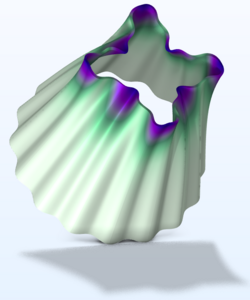
This example illustrates a linear buckling analysis conducted for a corrugated conical shell, utilizing a single sector of the geometry along with cyclic symmetry periodicity edge conditions. The results are compared to those using the full shell geometry. 詳細を見る
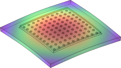
Flip chip (FC) is a widely used form of advanced semiconductor packaging that yields high interconnection density and good signal transmission performance of the semiconductor device as well as a reduction in size. In FC devices, the chip is placed face down and directly bonded to the ... 詳細を見る
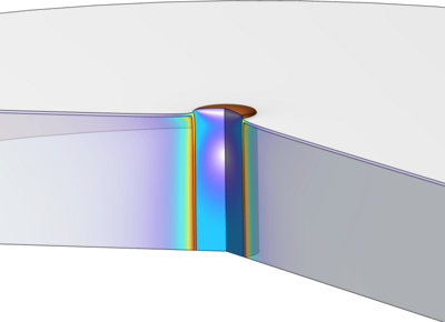
Through-silicon vias (TSVs) allow chips or wafers to be connected vertically, making TSV a crucial technology for 2.5D and 3D packaging. The basic structure of a TSV consists of a deep hole penetrating a silicon substrate, a filling metal (usually copper) in the deep hole, and an ... 詳細を見る
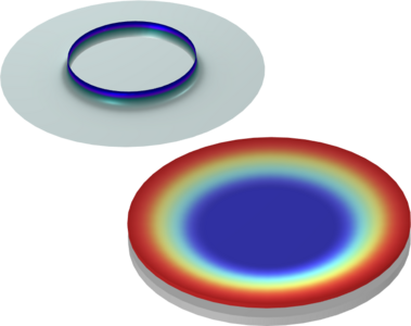
In direct bonding, the in-plane relative displacement between corresponding points on the bonding surfaces of the top and bottom wafers, denoted as IPD (In-Plane Distortion), is the primary yield killer in the bonding process. This model can predict the entire direct wafer bonding ... 詳細を見る
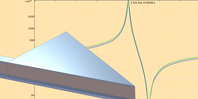
This model demonstrates how to extract the lumped parameters for an mBVD equivalent circuit from a FEM simulation and how to leverage such a model directly using the Electrical Circuit interface. A 3D layered FBAR resonator is considered as an example. Related Blog Post Leveraging the ... 詳細を見る
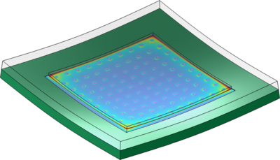
Flip-chip (FC) is one of the advanced forms of semiconductor device packaging that is widely used in today's semiconductor packages for its capability to minimize packaging size while enhancing electrical interconnection density and transmission performance. In FC devices, the active ... 詳細を見る