FSI Analysis of Wafer-to-Wafer (W2W) Direct Bonding Process
Application ID: 151871
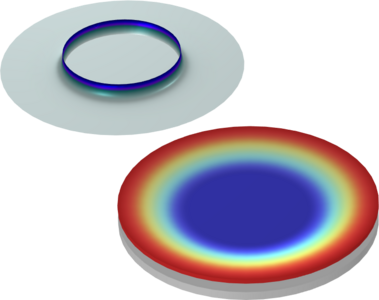
In direct bonding, the in-plane relative displacement between corresponding points on the bonding surfaces of the top and bottom wafers, denoted as IPD (In-Plane Distortion), is the primary yield killer in the bonding process. This model can predict the entire direct wafer bonding process: wafer flattening, downward pressing contact, bonding wave propagation, and load removal. Ultimately, it provides the W2W bonding wave velocity, IPD, warpage, and stress distribution under different process parameters.
この model の例は, 通常次の製品を使用して構築されるこのタイプのアプリケーションを示しています.
ただし, これを完全に定義およびモデル化するには, 追加の製品が必要になる場合があります. さらに, この例は, 次の製品の組み合わせのコンポーネントを使用して定義およびモデル化することもできます.
アプリケーションのモデリングに必要な COMSOL® 製品の組み合わせは, 境界条件, 材料特性, フィジックスインターフェース, パーツライブラリなど, いくつかの要因によって異なります. 特定の機能が複数の製品に共通している場合もあります. お客様のモデリングニーズに適した製品の組み合わせを決定するために, 製品仕様一覧 を確認し, 無償のトライアルライセンスをご利用ください. COMSOL セールスおよびサポートチームでは, この件に関するご質問にお答えしています.