
Consistent 3-D Modeling of Eddy Currents and Electric Field in Package Sealing Inductors
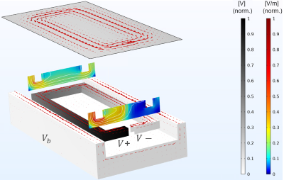
A three‑dimensional modeling approach for the consistent computation of eddy currents and electric field in inductor devices used in package sealing applications is presented. Eddy currents induced in the thin aluminum layer of the packaging material lead to Joule heating and enable induction sealing; however, under high‑frequency and high‑current operation, substantial voltage drop and correspondingly high electric field can arise, possibly compromising device insulation owing to electrical discharges. Although breakdown phenomena are diverse and complex, requiring a deeper understanding of the electronic processes involved, electric field modeling represents the first step toward their assessment. Nevertheless, for a realistic representation of the electric field, its computation must be consistent with inductive phenomena. The proposed model aims to solve eddy currents and electric field in a fully consistent manner. The model is implemented using the Electric and Magnetic Fields interface of the AC/DC Module, where both the electrostatic potential and the magnetic vector potential are solved simultaneously. In the device, the relatively thick coil and body conductors are modeled using an “Impedance Boundary Condition” (IBC), while the thin workpiece is represented through a "Surface Current Density” (SCD) feature. SCD is adopted instead of the (more general) “Transition Boundary Condition” (TBC) since TBC was found to lead to ill‑conditioned systems that cannot be solved even with robust direct solvers such as MUMPS. By contrast, SCD is well suited to the present problem since the workpiece thickness is much smaller than the skin depth at the operating frequency, and its application results in improved numerical properties of the system matrix. A magnetodielectric material (magnetic and electrically insulating) completes the device. Modeled using the “Ampère’s Law in Solids” feature, it guides the magnetic flux density toward the workpiece, improving efficiency and electrically insulating the coil from the body. The electric field within the magnetodielectric is critical, since breakdown in magnetodielectric lead to inductor failure. The self‑consistent computation of electrostatic potential and magnetic vector potential allows accounting for both voltage drop and current density distributions on the conductors. This avoids oversimplified electrostatic approximations that fail to capture localized high‑field regions (such as those at coil terminals) and ensures consistency with inductive effects including proximity effects, which, in turn, influence the electric field distribution in the insulating material. Then, by means of this modeling approach, it is also possible to impose electrostatic potential boundary conditions at the input and output terminal edges of the coil IBC domain. This enables: (i) representation of experimental breakdown test conditions, where voltage is directly applied to the coil terminals; and (ii) discrimination between unbalanced and balanced circuit topologies. Balanced topologies are advantageous, since the coil‑to‑body voltage is halved, thereby reducing the electric field in the magnetodielectric, while the coil current is unaffected, and thus the magnitude of the induced eddy currents in the workpiece. In the paper, a simplified (dummy) inductor model is first used to illustrate the problem and validate the modeling approach. The methodology is then applied to a real inductor device used in industrial induction sealing applications.
ダウンロード
- 17401_final.pdf - 0.57MB


