Microlithography Lens
Application ID: 92221
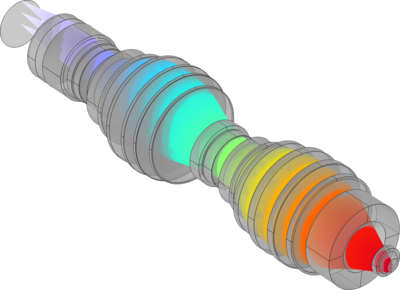
Microlithography lenses are used to project the image of an integrated circuit onto a silicon substrate. This tutorial demonstrates how to create a 21-element fused silica lens which has a NA of 0.56 which is designed to be used at a wavelength of 248nm. The lens, which has a total length of 1 meter, has a magnification of -0.25 with excellent image quality over a 23.4mm image circle.
この model の例は, 通常次の製品を使用して構築されるこのタイプのアプリケーションを示しています.
ただし, これを完全に定義およびモデル化するには, 追加の製品が必要になる場合があります. さらに, この例は, 次の製品の組み合わせのコンポーネントを使用して定義およびモデル化することもできます.
アプリケーションのモデリングに必要な COMSOL® 製品の組み合わせは, 境界条件, 材料特性, フィジックスインターフェース, パーツライブラリなど, いくつかの要因によって異なります. 特定の機能が複数の製品に共通している場合もあります. お客様のモデリングニーズに適した製品の組み合わせを決定するために, 製品仕様一覧 を確認し, 無償のトライアルライセンスをご利用ください. COMSOL セールスおよびサポートチームでは, この件に関するご質問にお答えしています.