Modeling Argon Ion Sputtering on a Silicon Surface
Application ID: 140971
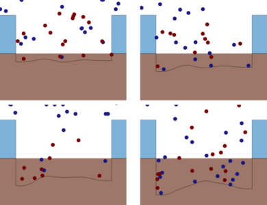
Ion beam etching is a critical technique widely used in semiconductor manufacturing, materials science, and microelectromechanical systems (MEMS). This proof-of-concept model simulates argon ion sputtering of a silicon surface using the Charged Particle Tracing interface. A Deformed Geometry interface is used to capture sputter-driven surface evolution, enabling visualization and analysis of morphology changes.
Check out our accompanying blog post on this model: “Modeling Argon Sputtering on a Silicon Surface”.
この model の例は, 通常次の製品を使用して構築されるこのタイプのアプリケーションを示しています.
ただし, これを完全に定義およびモデル化するには, 追加の製品が必要になる場合があります. さらに, この例は, 次の製品の組み合わせのコンポーネントを使用して定義およびモデル化することもできます.
アプリケーションのモデリングに必要な COMSOL® 製品の組み合わせは, 境界条件, 材料特性, フィジックスインターフェース, パーツライブラリなど, いくつかの要因によって異なります. 特定の機能が複数の製品に共通している場合もあります. お客様のモデリングニーズに適した製品の組み合わせを決定するために, 製品仕様一覧 を確認し, 無償のトライアルライセンスをご利用ください. COMSOL セールスおよびサポートチームでは, この件に関するご質問にお答えしています.