Phase Delay of a SOI Tapered Waveguide
Application ID: 151161
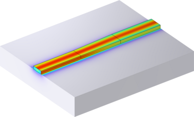
A small building block of integrated photonics, i.e., a Silicon-on-Insulator taper, is considered. For a larger system design, it might be useful to determine the phase delay such a device introduces.
Here, we showcase the layout needed to do it in COMSOL, including a proper Port placement, its phase correction, and manual phase extraction.
We also touch on the way a 3D Frequency Domain simulation correlates with a 2D Boundary Mode Analysis and analytic Transfer Matrix Method considerations. This also provides us with an option to validate the finite element model.
この model の例は, 通常次の製品を使用して構築されるこのタイプのアプリケーションを示しています.
ただし, これを完全に定義およびモデル化するには, 追加の製品が必要になる場合があります. さらに, この例は, 次の製品の組み合わせのコンポーネントを使用して定義およびモデル化することもできます.
アプリケーションのモデリングに必要な COMSOL® 製品の組み合わせは, 境界条件, 材料特性, フィジックスインターフェース, パーツライブラリなど, いくつかの要因によって異なります. 特定の機能が複数の製品に共通している場合もあります. お客様のモデリングニーズに適した製品の組み合わせを決定するために, 製品仕様一覧 を確認し, 無償のトライアルライセンスをご利用ください. COMSOL セールスおよびサポートチームでは, この件に関するご質問にお答えしています.