Photonic Crystal
Application ID: 14703
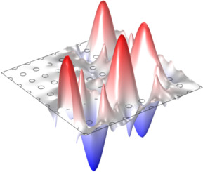
Photonic crystal devices are periodic structures of alternating layers of materials with different refractive indices. Waveguides that are confined inside of a photonic crystal can have very sharp low-loss bends, which may enable an increase in integration density of several orders of magnitude. This is a study of a photonic crystal waveguide. The crystal features a grid of GaAs pillars. Depending on the distance between the pillars, waves within a certain frequency range will be reflected instead of propagating through the crystal. This frequency range is called the photonic band gap. When some of the GaAs pillars in the crystal structure are removed, a guide for the frequencies within the band gap is created. Light can then propagate along the outlined guide geometry.
この model の例は, 通常次の製品を使用して構築されるこのタイプのアプリケーションを示しています.
ただし, これを完全に定義およびモデル化するには, 追加の製品が必要になる場合があります. さらに, この例は, 次の製品の組み合わせのコンポーネントを使用して定義およびモデル化することもできます.
アプリケーションのモデリングに必要な COMSOL® 製品の組み合わせは, 境界条件, 材料特性, フィジックスインターフェース, パーツライブラリなど, いくつかの要因によって異なります. 特定の機能が複数の製品に共通している場合もあります. お客様のモデリングニーズに適した製品の組み合わせを決定するために, 製品仕様一覧 を確認し, 無償のトライアルライセンスをご利用ください. COMSOL セールスおよびサポートチームでは, この件に関するご質問にお答えしています.