Reflow soldering in IC packaging
Application ID: 120151
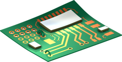
Reflow soldering is an important process in IC packaging. In reflow soldering, the solder materials are melted to create joints between electrical components and the PCBs for structural and electrical connections.
This model demonstrates the process of attaching chips to a PCB by reflow soldering. The model is implemented using the “Activation” feature. Due to different thermal expansion coefficients of the materials, residual stresses remain in the final product. This leads to warpage of the PCB and stress concentration in the solder joints.
In this model, the temperature change is described by a user-defined function. For further extension, the heat transfer between the structure and the surroundings can be considered to obtain detailed temperature distribution and evolution. In addition, more complex constitutive models such as viscoplasticity models can be applied for the behavior of solder materials at high temperature.
この model の例は, 通常次の製品を使用して構築されるこのタイプのアプリケーションを示しています.
ただし, これを完全に定義およびモデル化するには, 追加の製品が必要になる場合があります. さらに, この例は, 次の製品の組み合わせのコンポーネントを使用して定義およびモデル化することもできます.
アプリケーションのモデリングに必要な COMSOL® 製品の組み合わせは, 境界条件, 材料特性, フィジックスインターフェース, パーツライブラリなど, いくつかの要因によって異なります. 特定の機能が複数の製品に共通している場合もあります. お客様のモデリングニーズに適した製品の組み合わせを決定するために, 製品仕様一覧 を確認し, 無償のトライアルライセンスをご利用ください. COMSOL セールスおよびサポートチームでは, この件に関するご質問にお答えしています.