アプリケーションギャラリには電気, 構造, 音響, 流体, 熱および化学分野に関連する COMSOL Multiphysics® チュートリアルおよびデモアプリファイルが用意されています. これらの例はチュートリアルモデルまたはデモアプリファイルとそれに付随する手順をダウンロードすることにより独自のシミュレーション作業の開始点として使用できます.
クイック検索機能を使用して専門分野に関連するチュートリアルやアプリを検索します. MPHファイルをダウンロードするには, ログインするか, 有効な COMSOL ライセンスに関連付けられている COMSOL Access アカウントを作成します. ここで取り上げた例の多くは COMSOL Multiphysics® ソフトウェアに組み込まれ ファイルメニューから利用できるアプリケーションライブラリからもアクセスできることに注意してください.
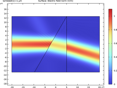
This model illustrates the refraction of light while passing through an optical prism using s– and p–polarized incident Gaussian beams. The prism boundaries are coated with anti–reflection coatings. It also calculates the reflectance and transmittance to analyze the performance of anti ... 詳細を見る
The thermal effects of a laser beam incident on a Semiconductor Saturable Absorber Mirror (SESAM) are simulated under a range of incident beam powers. This is done in two steps. The first study simulates the multiphysics combination of the saturated absorption of the beam on a SESAM, ... 詳細を見る
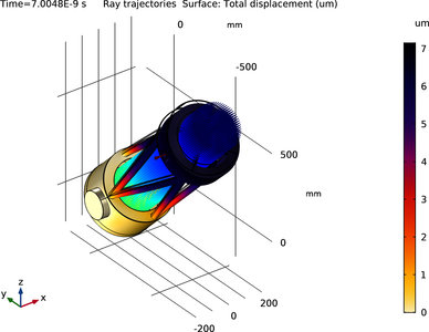
This tutorial demonstrates a structural analysis of a simple telescope. The deformation of the telescope structure under gravity is examined and the effect on image quality is demonstrated. 詳細を見る
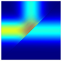
A beam splitter is used to split a single beam of light into two. One way of making a splitter is to deposit a thin layer of metal between two glass prisms. The beam is slightly attenuated within the layer, and split into two paths. In this example, the thin metal layer is modeled using ... 詳細を見る

This model demonstrates the use of boundary element method in the Electromagnetic Waves, Boundary Element interface to model an optical Yagi-Uda antenna. The antenna is driven by an electrical point dipole, which is implemented through the background field. The field distribution around ... 詳細を見る
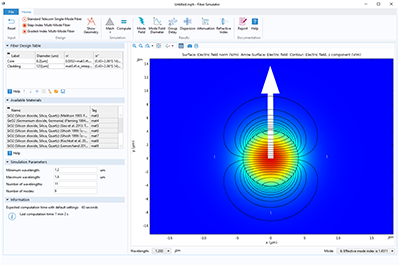
The transmission speed of optical waveguides is superior to microwave waveguides because optical devices have a much higher operating frequency than microwaves, enabling a far higher bandwidth. Single-mode step-index fibers are used for long-haul (even transoceanic) communication, ... 詳細を見る
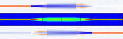
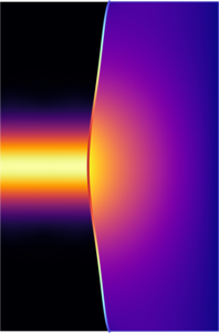
Focusing a laser beam onto the tip of a single mode fiber is a common way to couple light. To achieve good coupling efficiency, the spatial mode of the light field has to match the spatial mode of the fiber. In this model, we use the beam envelopes method to compute a small free-space ... 詳細を見る

Photonic crystal devices are periodic structures of alternating layers of materials with different refractive indices. Waveguides that are confined inside of a photonic crystal can have very sharp low-loss bends, which may enable an increase in integration density of several orders of ... 詳細を見る
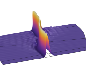
This model demonstrates how to simulate the propagation of guided waves in a dielectric S-bent optical waveguide. The model demonstrates that the phase approximation, required by the Electromagnetic Waves, Beam Envelopes interface, can be numerically calculated by solving an additional ... 詳細を見る
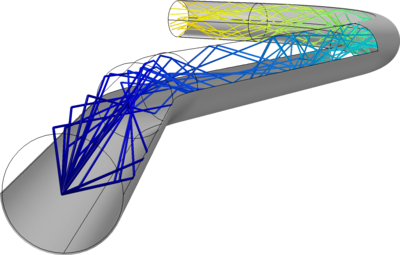
Light pipes are structures that can be used to transport light between different locations. In general, they can be divided into two major groups: tubes lined with a reflective coating and transparent solids that contain light via total internal reflection. In this tutorial, light is ... 詳細を見る