Stress–Optical Effects in a Photonic Waveguide
Application ID: 190
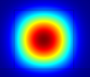
Planar photonic waveguides in silica (SiO2) have great potential for use in wavelength routing applications. The major problem with this type of waveguide is birefringence. Anisotropic refractive indices result in fundamental mode splitting and pulse broadening. The goal is to minimize birefringence effects by adapting materials and manufacturing processes. One source of birefringence is the use of a silicon (Si) wafer as the substrate onto which the waveguide structure is deposited.
After annealing at high temperatures, a mismatch in thermal expansion between the silica and silicon layers results in thermally induced stresses in the structure at the operating temperature (typically room temperature).
この model の例は, 通常次の製品を使用して構築されるこのタイプのアプリケーションを示しています.
ただし, これを完全に定義およびモデル化するには, 追加の製品が必要になる場合があります. さらに, この例は, 次の製品の組み合わせのコンポーネントを使用して定義およびモデル化することもできます.
- COMSOL Multiphysics® and
- 波動光学モジュール and
- either the MEMS モジュール, or 構造力学モジュール
アプリケーションのモデリングに必要な COMSOL® 製品の組み合わせは, 境界条件, 材料特性, フィジックスインターフェース, パーツライブラリなど, いくつかの要因によって異なります. 特定の機能が複数の製品に共通している場合もあります. お客様のモデリングニーズに適した製品の組み合わせを決定するために, 製品仕様一覧 を確認し, 無償のトライアルライセンスをご利用ください. COMSOL セールスおよびサポートチームでは, この件に関するご質問にお答えしています.